# Combinational Logic
Recall that we are disciplining ourselves to design synchronous sequential circuits, which consist of combinational logic and registers. The outputs of combinational logic depend only on the current inputs. This section describes how to write **behavioral** models of combinational logic with HDLs.
## Bitwise Operators
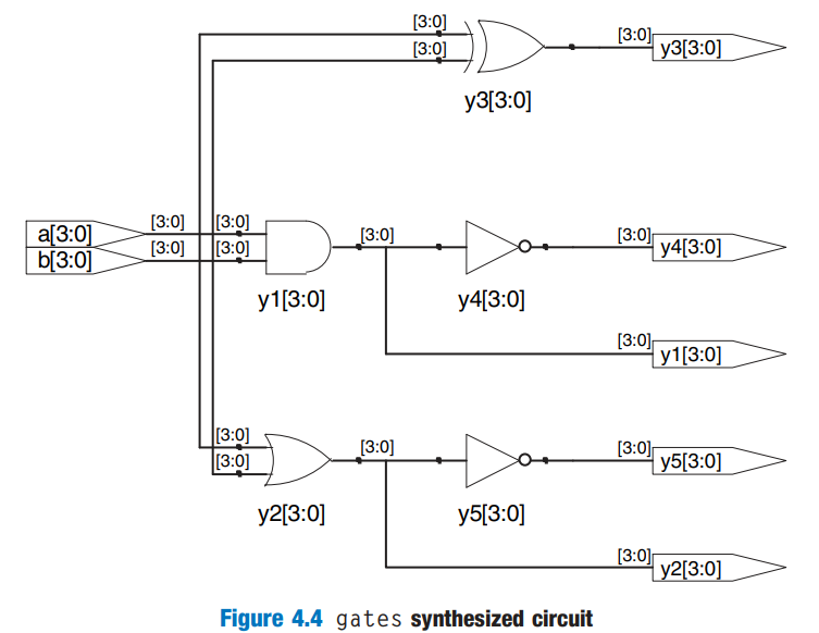
*Bitwise* Operators act on **single-bit** signals or on **multi-bit** busses. For example, the `gates` module in HDL Example 4.3 demonstrates bitwise operations on 4-bit busses for most common basic logic functions.
{% tabs %}
{% tab title="SystemVerilog" %}
{% code title="Example 4.3 Logic Gates" lineNumbers="true" %}
```verilog
module gates(input logic [3:0] a, b,
output logic [3:0] y1, y2, y3
y4, y5, y6);
/* five different two-input logic
gates acting on 4-bit busses */
assign y1 = a & b; // AND
assign y2 = a | b; // OR
assign y3 = a ^ b; // XOR
assign y4 = ~(a ^ b); // XNOR
assign y5 = ~(a & b); // NAND
assign y6 = ~(a | b); // NOR
endmodule
```
{% endcode %}
{% endtab %}
{% tab title="Verilog" %}
{% code title="Example 4.3 Logic Gates" lineNumbers="true" %}
```verilog
module gates(input [3:0] a, b,
output [3:0] y1, y2, y3
y4, y5, y6);
/* Five different two-input logic
gates acting on 4 bit busses */
assign y1 = a & b; // AND
assign y2 = a | b; // OR
assign y3 = a ^ b; // XOR
assign y4 = ~(a ^ b); // XNOR
assign y5 = ~(a & b); // NAND
assign y6 = ~(a | b); // NOR
endmodule
```
{% endcode %}
{% endtab %}
{% endtabs %}
The schematic for the above code snippet may look like as follows,
### Operators, Operands, Expression and Statements
Using the `gate` module shown in Example 4.3,
1. `~`, `^`, `|` are examples of SystemVerilog/Verilog *operators*.
2. `a`, `b`, and `y1` are *operands*
3. A combination of operators and operands, such as `a & b`, `~(a | b)`, is called an *expression*
4. A complete command such as `assign y4 = ~(a & b);` is called a *statement*
### Continuous Assignment Statement
`assign out = in1 op in2;` is called a *continuous assignment statement*. Continuous assignment statements end with a semicolon. Anytime the inputs on the right side of the `=` in a continuous assignment state change, the output on the left side is recomputed. Thus, continuous assignment statements describe combinational logic.
## Comments and White Space
SystemVerilog/Verilog comments are just like those in C or Java. SystemVerilog/Verilog is case-sensitive. `y1` and `Y1` are different signals in SystemVerilog/Verilog.
SystemVerilog/Verilog is not picky about the use of white space (e.g., spaces, tabs, and line breaks). Nevertheless, proper indenting and use of blank lines is helpful to make nontrivial designs readable.
{% hint style="info" %}
Be consistent in your use of capitalization and underscores in signal and module names. This text uses all lower case. Module and signal names must not begin with a digit.
{% endhint %}
## Reduction Operators
Reduction operators imply a multiple-input gate acting on a single bus. HDL Example 4.4 describes an eight-input AND gate with inputs $$a\_7,a\_6,\cdots,a\_0$$.
{% tabs %}
{% tab title="SystemVerilog" %}
{% code title="Example 4.4 Eight-Input AND" lineNumbers="true" %}
```verilog
module and8(input logic [7:0] a,
output logic y);
assign y = &a;
// &a is much easier to write than
// assign y = a[7] & a[6] & a[5] & a[4] &
// a[3] & a[2] & a[1] & a[0];
endmodule
```
{% endcode %}
{% endtab %}
{% tab title="Verilog" %}
{% code title="Example 4.4 Eight-Input AND" lineNumbers="true" %}
```verilog
module and8(input [7:0] a,
output y);
assign y = &a;
// &a is much easier to write than
// assign y = a[7] & a[6] & a[5] & a[4] &
// a[3] & a[2] & a[1] & a[0];
endmodule
```
{% endcode %}
{% endtab %}
{% endtabs %}
Analogous reduction operators exist for OR, XOR, NAND, and XNOR gates. Recall that a multiple-input XOR performs **parity**, returning TRUE if an odd number of inputs are TRUE.
## Conditional Assignment
*Conditional Assignments* select the output from among alternatives based on an input called the *condition*. This is pretty useful for describing the **multiplexer** in combinational logic.
{% stepper %}
{% step %}
**2:1 multiplexer**
HDL Example 4.5 illustrates a 2:1 multiplexer using conditional assignment.
{% tabs %}
{% tab title="SystemVerilog" %}
{% code title="Example 4.5 2:1 Multiplexer" lineNumbers="true" %}
```verilog
module mux2(input logic [3:0] d0, d1,
input logic s,
output logic [3:0] y);
assign y = s ? d1 : d0;
endmodule
```
{% endcode %}
{% hint style="success" %}
#### Code Explanation
1. `? :` is especially useful for describing a multiplexer because, based on the first input, it selects between two others.
2. `? :` is also called a *ternary operator*, which is same to C and Java.
{% endhint %}
{% endtab %}
{% tab title="Verilog" %}
{% code title="Example 4.5 2:1 Multiplexer" lineNumbers="true" %}
```verilog
module mux2(input [3:0] d0, d1,
input s,
output [3:0] y);
assign y = s ? d1 : d0;
endmodule
```
{% endcode %}
{% endtab %}
{% endtabs %}
{% endstep %}
{% step %}
**4:1 Multiplexer**
HDL Example 4.6 shows a 4:1 multiplexer based on the same principle as the 2:1 multiplexer in HDL Example 4.5.
{% tabs %}
{% tab title="SystemVerilog" %}
{% code title="Example 4.6 4:1 Multiplexer" lineNumbers="true" %}
```verilog
module mux4(input logic [3:0] d0, d1, d2, d3,
input logic [1:0] s,
output logic [3:0] y);
assign y = s[1] ? (s[0] ? d3 : d2)
: (s[0] ? d1 : d0);
endmodule
```
{% endcode %}
{% endtab %}
{% tab title="Verilog" %}
{% code title="Example 4.6 4:1 Multiplexer" lineNumbers="true" %}
```verilog
module mux4(input [3:0] d0, d1, d2, d3,
input [1:0] s,
output [3:0] y);
assign y = s[1] ? (s[0] ? d3 : d2)
: (s[0] ? d1 : d0);
endmodule
```
{% endcode %}
{% endtab %}
{% endtabs %}
{% endstep %}
{% endstepper %}
## Internal Variables
*Internal Variables* refer to the variables that are neither inputs nor outputs but are used only internal to the module. They are similar to local variables in programming languages. Example 4.7 shows how they are used in HDLs.
{% tabs %}
{% tab title="SystemVerilog" %}
{% code title="Example 4.7 Full Adder" lineNumbers="true" %}
```verilog
module fulladder(input logic a, b, cin,
output logic s, cout);
logic p, g;
assign p = a ^ b;
assign g = a & b;
assign s = p ^ cin;
assign cout = g | (p & cin);
endmodule
```
{% endcode %}
{% hint style="success" %}
#### Code Explanation
1. In this example, the signal `p` and `g` are two **internal variables.**
2. HDL assignments (`assign` in SystemVerilog/Verilog) take place **concurrently**. This is different from conventional programming language like C or Java. In HDL, the order of statements doesn't matter.
{% endhint %}
{% endtab %}
{% tab title="Verilog" %}
{% code title="Example 4.7 Full Adder" lineNumbers="true" %}
```verilog
module fulladder(input a, b, cin,
output s, cout);
wire p, g;
assign p = a ^ b;
assign g = a & b;
assign s = p ^ cin;
assign cout = g | (p & cin);
endmodule
```
{% endcode %}
{% hint style="success" %}
#### Code Explanation
1. In Verilog, *wires* are used to represent internal variables whose values are defined by `assign` statements such as `assign p = a ^ b`.
2. Wires technically have to be declared only for multibit busses, but it is good practice to include them for all internal variables; their declaration could have been ommited in this example.
{% endhint %}
{% endtab %}
{% endtabs %}
## Precedence
Table 4.1 summarises the operator precedence in SystemVerilog
## Numbers
Numbers can be specified in binary, octal, decimal, or hexadecimal (bases 2, 8, 10, and 16, respectively).
* The size, e.g., the number of bits, may optionally be given, and leading zeros are inserted to reach this size.
* Underscores (`_`) in numbers are ignored and can be helpful in breaking long numbers into more readable chunks.
The following table shows numbers are written in SystemVerilog/Verilog.
| Numbers | Bits | Base | Val | Stored |
| -------------- | ---- | ---- | --- | -------------- |
| `3'b101` | 3 | 2 | 5 | 101 |
| `'b11` | ? | 2 | 3 | 000 ... 0011 |
| `8'b11` | 8 | 2 | 3 | 00000011 |
| `8'b1010_1011` | 8 | 2 | 171 | 10101011 |
| `3'd6` | 3 | 10 | 6 | 110 |
| `6'o42` | 6 | 8 | 34 | 100010 |
| `8'hAB` | 8 | 16 | 171 | 10101011 |
| `42` | ? | 10 | 42 | 00 ... 0101010 |
{% hint style="success" %}
#### Table Explanation
1. It is a better practice to explicitly give the size of the numbers.
2. An exception is that, `0` and `1` are SystemVerilog idioms for filling a bus with all 0s and all 1s, respectively.
{% endhint %}
### Z's and X's
HDLs use `z` to indicate a floating value, `z` is particularly useful for describing a tristate buffer, whose output floats when the enable is 0. Similarly, HDLs use `x` to indicate an invalid logic level.
> **TODO:** Read through tristate buffer if have time.
{% hint style="warning" %}
Seeing `x` (SystemVerilog/Verilog) or `u` (VHDL) values in simulation is almost always an indication of a bug or bad coding practice.
{% endhint %}
## Bit Swizzling
Often it is necessary to operate on a subset of a bus or to concatenate (join together) signals to form busses. These operations are collectively known as *bit swizzling*. In HDL Example 4.12, `y` is given the 9-bit value $$c\_2c\_1d\_0d\_0d\_0d\_0c\_0101$$ using bit swizzling operations.
{% code title="Example 4.12 Bit Swizzling" lineNumbers="true" %}
```verilog
assign y = {c[2:1], {3{d[0]}}, c[0], 3'b101};
```
{% endcode %}
## Delays
HDL statements may be associated with delays specified in arbitrary units. They are helpful during simulation to predict how fast a circuit will work (if you specify meaningful delays) and also for debugging purposes to understand cause and effect (deducing the source of a bad output is tricky if all signals change simultaneously in the simulation results).
{% hint style="warning" %}
These delays are ignored during synthesis! Thus, it is highly **not recommended** to use delays in combinational circuits in RTL! However, delays may be very useful in [testbench](https://wenbo-notes.gitbook.io/ddca-notes/textbook/hardware-description-languages/testbench)!
{% endhint %}
The delay of a gate produced by the synthesizer depends on its $$t\_{\text{pd}}$$ and $$t\_{\text{cd}}$$ specifications, not on numbers in HDL code.
HDL Example 4.13 adds delays to the original function from HDL Example 4.1, $$y=\bar a\bar b\bar c+a\bar b\bar c+a\bar bc$$.
{% tabs %}
{% tab title="SystemVerilog" %}
{% code title="Example 4.13 Logic Gates with Delays" lineNumbers="true" %}
```verilog
`timescale 1ns/1ps
module example(input logic a, b, c,
output logic y);
logic ab, bb, cb, n1, n2, n3;
assign #1 {ab, bb, cb} = ~{a, b, c};
assign #2 n1 = ab & bb & cb;
assign #2 n2 = a & bb & cb;
assign #2 n3 = a & bb & c;
assign #4 y = n1 | n2 | n3;
endmodule
```
{% endcode %}
{% endtab %}
{% tab title="Verilog" %}
{% code title="Example 4.13 Logic Gates with Delays" lineNumbers="true" %}
```verilog
`timescale 1ns/1ps
module example(input a, b, c,
output y);
wire ab, bb, cb, n1, n2, n3;
assign #1 {ab, bb, cb} = ~{a, b, c};
assign #2 n1 = ab & bb & cb;
assign #2 n2 = a & bb & cb;
assign #2 n3 = a & bb & c;
assign #4 y = n1 | n2 | n3;
endmodule
```
{% endcode %}
{% endtab %}
{% endtabs %}
{% hint style="success" %}
#### Code Explanation
1. SystemVerilog/Verilog can include a timescale directive that indicates the value of each time unit. The statement is of the form `timescale unit/precision`. In this file, each unit is 1 ns, and the simulation has 1 ps precision.
2. If no timescale directive is given in the file, a default unit and precision (usually 1 ns for both) is used.
{% endhint %}